Chip Scale Package
CABGA

Description
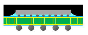
Amkor의 ChipArray®BGA (CABGA)는 Laminate를 기판으로 사용하는 package로, SMT 실장방식으로 보드와 연결됩니다. CABGA는 molded array family를 대표하는 package 용어로서도 쓰이며, 0.3mm 이상의 ball pitch / 1.5~27mm body / 0.5~1.5mm Max thickness로 다양한 product line을 제공합니다.
Features
- 1.5~27mm body size
- 4~700 ball counts
- 0.3~1.0mm ball pitch
Applications
- FPGAs, ASICS, Memory, Analog, RF, MCUs, …
- Mobile, gaming, notebook, PC, networking, …
Offerings
- Multi chip / Stacked die
- Passive component integration
- BGA / LGA
Reference
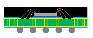
▲ Cross Section – CABGA
SCSP
Description
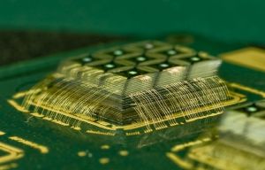
Stacked CSP (SCSP)는 CABGA를 생산하는 Amkor의 선도기술을 이용해서 chip을 적층해 구성하는 package입니다. SCSP는 high level의 silicon integration을 가능하게 하며 package 사이즈도 효과적으로 줄일 수 있습니다. Amkor에서는 40개의 die까지 적층 및 wire bonding 작업을 할 수 있습니다.
Features
- 4~21mm body size
- Package height down to 0.6mm
- Thin DA film and spacer technology
- Low loop wire bonding less than 45㎛
- Vacuum transfer and compression molding
Applications
- Mobile, Portable devices
Offerings
- Logic / Flash, Digital / Analog and other ASIC / Memory combinations
- Hybrid stack (flip chip + wire bonding)
- Passive component integration options
Reference
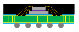
▲ Cross Section – 2+0
fcCSP
Description
Amkor는 CSP package 형태의 flip chip package를 제공합니다. Flip chip interconnect 기술은 기존의 wire bond interconnect를 대체하는 기술로 더욱 향상된 전기적 특성을 제공하며, 배선밀도증가 및 wire의 loop가 없어짐으로써 더 작은 사이즈의 package 구현이 가능합니다. 이러한 flip chip bump 형태는 area array와 peripheral 모두 가능하며, solder 혹은 Cu pillar bump도 선택해 적용할 수 있습니다.
Features
- 2~21mm body size
- 0.3~1.0mm ball pitch
- 9~1500 + ball counts
- 25/50㎛ staggered bump pitch with Cu pillar, TCNCP
Applications
- Handheld / portable devices
- Workstations, servers, data communication
- RF applications
Offerings
- Thin core laminate or build up substrate
- BGA or LGA format
- Hybrid stacked package (flip chip + wire bonding)
- Bare die, overmolded or exposed die format
- MR or TCNCP chip attach
Reference
▲ Cross Section – Single Chip