Advanced Package
PoP

Description
Amkor는 2004년에 Package Stackable very thin fine pitch BGA (PSvfBGA)를 처음 출시했습니다. Wire bonding technology가 flip chip으로 대체되면서 Package Stackable flip chip Chip Scale Package (PSfcCSP)로 얇은 flip chip die를 expose된 형태로 제공했습니다. Memory 구조 변화와 함께 higher density, height reduction 수용이 가능한 2세대 PoP가 탄생했는데, 이것이 TMV® (Through Mold Via)입니다. TMV 기술은 큰 die to package ratio를 갖는 device에서 얇은 substrate와 안정적인 bottom package를 제공합니다.
Features
- 10~15mm body size, additional sizes based on demand
- Wafer thinning / handling < 100㎛
- Stacked package height of 1.12~1.50mm available
- 0.35~1.0mm ball pitch (0.20mm memory pitch)
Applications
- Portable electronic products
- Baseband or application processor + combo memory
- Image processor + memory
- Audio / graphics processor + memory
Offerings
- Wire bonding
- Flip chip
- Hybrid stack (flip chip + wire bonding)
- Exposed die TMV
- Fan-in PoP (with interposer)
Reference

▲ Cross Section – TMV
SiP/Module
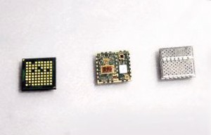
Description
System-in-Package (SiP)는 하나 혹은 그 이상의 IC (Integrated Circuit) 조합으로 구성되며, passive component나 MEMS를 포함할 수 있고, package 내에서 하나의 system 혹은 sub-system으로 동작하는 package를 말합니다. 즉, 하나 이상의 IC chip과 더불어 기존에는 Motherboard에 장착되었던 다른 component들이 함께 구현됩니다. Component들에는 surface mount discrete passive, Integrated Passive Networks (IPN), Integrated Passive Devices (IPD), SAW/BAW filters, EMI shields 등이 있습니다.
Features
- Smaller size solution than individually-packaged ICs
- Higher performance through shorter interconnect paths
- Lower overall cost of ownership
- Reduced time to market
Applications
- RF and wireless devices
- IoT or wearable
Offerings
- Cavity or recessed substrate
- Embedded passive or active device in a substrate
- POG (Passive On Glass)
- Double side assembly, POSSUM die
- Conformal / compartment shield
Reference

▲ Cross Section – SiP
WLCSP
Description
Amkor는 device와 end product의 Motherboard를 solder interconnection을 통해 직접 연결하는 Wafer Level Chip Scale Package (WLCSP)를 제공합니다. WLCSP는 wafer bumping (pad layer redistribution, RDL 포함 가능)을 비롯해 wafer level final test, device singulation 및 packing에 이르는 turnkey solution을 제공합니다. WLCSP는 mobile device의 성장과 더불어 small package와 lower cost에 대한 수요가 커지면서 빠르게 확장하고 있습니다.
Features
- 4~196 ball counts
- 0.3~1.0mm ball pitch
- PBO & Polyimide (PI) repassivation and RDL available
- Reliable thick Cu UBM or NiAu for best in class EM
performance
Applications
- High end RF WLAN
- FPGAs, power management
- Flash / EEPROM
- Integrated passive network
- Standard analog
Offerings
- Bump on Repassivation or bump on RDL
- CSPnl, CSPn2, CSPn3
- Molded option (CSPml, CSPm2)
Reference

▲ Cross Section – WLCSP